Home › Hardware› Chip Packaging Race Intensifies as AI Demand Strains Advanced Assembly Capacity
HardwareChip Packaging Race Intensifies as AI Demand Strains Advanced Assembly Capacity
Jordan Ellis
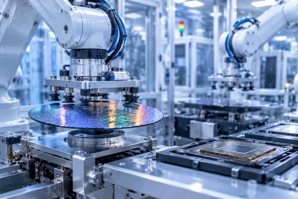
Advanced chip packaging has become a front-line constraint in the AI hardware supply chain, as foundries and assembly providers race to add capacity for complex techniques that stitch together high-bandwidth memory and logic dies.
Advanced chip packaging has moved from a back-end afterthought to a front-line constraint in the AI hardware supply chain, as foundries and outsourced assembly and test providers race to add capacity for the complex techniques that stitch together high-bandwidth memory and logic dies. The shift is reshaping investment priorities across the semiconductor industry, with packaging lines now commanding attention once reserved for leading-edge wafer fabs.
The pressure traces back to the architecture of modern AI accelerators, which rely on packaging methods such as chip-on-wafer-on-substrate and 2.5D interposers to place memory stacks alongside compute dies at very short distances. These approaches deliver the bandwidth and power efficiency that AI workloads demand, but they are far harder to scale than conventional wire-bond packaging. Yields are sensitive to warpage, thermal stress and substrate availability, and each generation of accelerator tends to require tighter design rules than the last.
Equipment suppliers and materials vendors are responding with new tooling for fine-pitch bonding, hybrid bonding and panel-level processing, while substrate makers work to close a persistent supply gap for high-layer-count organic substrates. Foundries are also bringing more packaging steps in-house, blurring the traditional boundary between wafer fabrication and assembly. For chip designers, the practical consequence is that packaging choices now influence performance, cost and time-to-market as much as process node selection does, and early engagement with assembly partners has become a scheduling necessity rather than an afterthought.
Long lead times and a thin bench of qualified engineers
Industry executives and analysts describe packaging as the discipline where the AI buildout is most likely to encounter friction over the next several quarters. They point to long lead times for advanced substrates and bonding tools, limited numbers of qualified engineers, and the difficulty of transferring processes from development lines to high-volume manufacturing. Several firms have said they are expanding packaging capacity and deepening partnerships with assembly houses, while cautioning that new lines take time to qualify and ramp. Analysts note that the investment is broad-based, spanning foundries, OSATs, substrate suppliers and equipment makers, which suggests the constraint is structural rather than a short-term mismatch.
The engineering bottleneck is not only a matter of headcount. Process recipes for 2.5D interposers and hybrid bonding demand tight control over alignment, cleanliness and thermal expansion, and those skills are built through years of hands-on work on development lines rather than acquired quickly. That makes the transfer from pilot production to high-volume output a delicate step, one that companies cannot easily compress by throwing money at new equipment alone.
Hybrid bonding, panel-level processing and the standards question
Attention now turns to capacity additions scheduled to come online over the coming year and whether they will ease the tightest links in the chain. Hybrid bonding is expected to move from niche deployment toward broader use, and panel-level packaging is being watched as a route to higher throughput and lower cost per unit. Standards work around chiplet interfaces and test methods could also reduce integration friction, though adoption will depend on coordination across competing vendors. For now, the industry’s ability to scale advanced packaging will help determine how quickly AI hardware can be delivered, making assembly and test a strategic battleground rather than a commodity step.
Substrate availability remains a particular concern, since high-layer-count organic substrates require long qualification cycles and specialized production capacity that cannot be switched on overnight. Suppliers are investing in new lines, but the gap between announced capacity and qualified output is likely to persist through the near term. Panel-level processing, meanwhile, promises economies of scale by moving away from round wafers toward larger rectangular formats, but it requires new tooling and fresh process development across the supply chain.
For foundries, the strategic calculus has shifted. Packaging was once a step farmed out to assembly partners with little involvement from wafer fabs; now, leading manufacturers are integrating more of the flow to protect yields and secure allocation for their largest customers. That integration raises questions about how much capacity will remain available to fabless chip designers who depend on merchant assembly houses, and whether smaller players will find themselves queued behind the largest AI accelerator programs.
The competitive dynamics extend to equipment makers as well, where demand for fine-pitch bonding tools and inspection systems has surged. Vendors are expanding production, but delivery schedules for specialized bonders remain stretched, and each tool must be matched to a customer’s specific process flow. Analysts caution that capacity additions announced today will not translate into usable output until qualification is complete, a process that can take multiple quarters for advanced nodes.
Standards efforts around chiplet interfaces could ease some of the integration burden by allowing dies from different vendors to be assembled more predictably, but progress depends on cooperation among companies that compete fiercely in other areas. Test methods for known-good dies are another unresolved piece, since packaging a defective die wastes an entire expensive assembly. Until those questions are settled, the industry’s ability to scale advanced packaging will help determine how quickly AI hardware can be delivered, making assembly and test a strategic battleground rather than a commodity step.
Read next

Hardware
Data Centre Operators Confront Power Crunch as AI Loads Surge in Singapore
Singapore's data centre operators are turning to liquid cooling and on-site generation as AI workloads push power density

AI
Banks Rethink Model Hosting as AI Workloads Strain On-Premise Infrastructure
Financial institutions are shifting from on-premise AI model hosting to hybrid architectures, balancing latency, data sovereignty, and cost

Security
Enterprise Ransomware Defense Shifts to Identity-First Playbooks as Attackers Target Credentials
Enterprise ransomware defense is shifting from perimeter controls to identity-first playbooks as attackers increasingly use stolen credentials to